Change the surface property of the patch to perfect electric conductor
(PEC).
Change the face of the patch to PEC.
In the 3D view, left-click on the patch face
repeatedly until the face is highlighted in yellow.
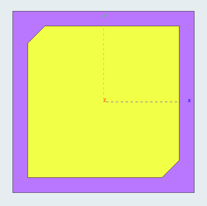
Figure 1. Top view of patch and substrate. The yellow highlighting
indicates that the patch face is selected.
From the right-click context menu, select
Properties.
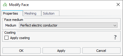
On the Modify Face dialog
(Properties tab), set the
Medium to Perfect electric
conductor.
Figure 2. The Modify Face dialog.
Click OK to change the face property and
to close the dialog.
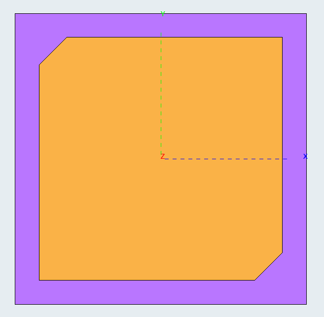
Figure 3. Top view showing the face of the patch set to PEC.
Change the face of the bottom substrate to PEC.
In the model tree, under
Union1, select
substrate.
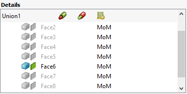
In the details tree, under
Faces, go through the list of faces. For each
face, click on to hide the face until only the bottom face of
the substrate remains.
Figure 4. Hidden items are greyed out when hidden in the 3D view.
From the right-click context menu, select
Properties.
On the Modify Face dialog
(Properties tab), set
Medium to Perfect electric
conductor.
Click OK to modify the face property and
to close the dialog.
Figure 5. Bottom view showing the bottom substrate face set to
PEC.
In the details tree, click on any of the faces.
From the right-click context menu, click
Show All to make faces visible again.
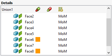
Note: The icon in the details tree indicate faces
set to PEC.
 to hide the face until only the bottom face of
the substrate remains.
to hide the face until only the bottom face of
the substrate remains.
 icon in the details tree indicate faces
set to PEC.
icon in the details tree indicate faces
set to PEC.