Creating the Model
Create the model in CADFEKO. Define any ports and sources required for the model. Specify the operating frequency or frequency range for the model.
- Set the model unit to millimetres.
-
Define the following variables.
- d1 = 2.22 (Distance between apertures.)
- d2 = 12.51 (Distance between apertures.)
- epsr = 2.2 (The relative permittivity of the substrate.)
- s = 10 (Length of the aperture.)
- w = 4.6 (Width of the microstrip.)
- strip_feed_arc_radius = 2*s (The radius of curved microstrip line.)
- strip_length = 2* s + d2 + d1 (The straight section length of the microstrip line.)
- substrate_depth = 50 (The substrate depth.)
- substrate_height = 1.58 (The substrate height.)
- substrate_width = 140 (The substrate width.)
- f_max = 5e9 (The maximum frequency.)
- f_min = 2.5e9 (The minimum frequency.)
-
Create a dielectric medium.
- Dielectric loss tangent: 0
- Relative permittivity: epsr
- Label: substrate
-
Create the straight section of the microstrip line.
-
Create a rectangle.
- Definition method: Base corner, width, depth
- Base corner (C): (0, -w/2, substrate_height)
- Width (W): strip_length
- Depth (D): w
-
Create a rectangle.
-
Create the feed section of the microstrip.
-
Create a rectangle.
- Definition method: Base corner, width, depth
- Base corner (C): (0, 0, 0)
- Width (W): w
- Depth (D): substrate_height
- On the Workplane tab set the Origin: (strip_length+strip_feed_arc_radius-w/2, strip_feed_arc_radius, 0)
-
Rotate the workplane of the rectangle 90° around
the U axis to align the rectangle in the XZ plane.
Tip: Right-click on the Origin box of the workplane and click Rotate workplane.
-
Create a rectangle.
-
Create the arc section of the microstrip.
-
Create an elliptic arc.
- Centre point (C): (strip_length, strip_feed_arc_radius, substrate_height)
- Radius (U): strip_feed_arc_radius + w/2
- Radius (V): strip_feed_arc_radius + w/2
- Start angle: -90
- Stop angle: 0
- Label: outer_circle
-
Create an elliptic arc.
-
Create a line.
- From: (0, -strip_feed_arc_radius-w/2, 0)
- To: (0, -strip_feed_arc_radius+w/2, 0)
- On the Workplane tab set the Origin: (strip_length, strip_feed_arc_radius, substrate_height
- Pathsweep Line1 on outer_circle.
-
Union all parts.
The resulting geometry represents half of the top microstrip section.
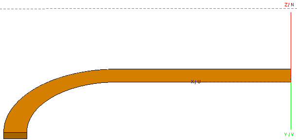
Figure 1. Geometry after Union operation. -
Copy and rotate Union1 by 180°
around the U axis.
Note: The new part represents half of the bottom microstrip.
-
Create the ground plate.
-
Create a rectangle.
- Base Corner (C): (0, -substrate_depth/2, 0)
- Width (W): substrate_width/2
- Depth (D): substrate_depth
- Label: ground_plate
-
Create a rectangle.
-
Create an aperture.
-
Create a rectangle.
- Base corner (C): (d2/2, -s/2, 0)
- Width (W):s
- Depth (D):s
- Label: aperture_1
-
Create a rectangle.
-
Create a second aperture.
-
Create a rectangle.
- Base corner (C): (d2/2+s+d1, -s/2, 0)
- Width (W):s
- Depth (D):s
- Label: aperture_2
-
Create a rectangle.
-
Subtract aperture_1 and
aperture_2 from ground_plate.
The resulting geometry is a ground plane between two microstrip lines with two square holes.
-
Copy and mirror all geometry around the VN plane.
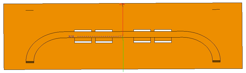
Figure 2. Geometry after the copy and mirror operation. - Union all the parts.
-
Set all faces to perfect electric conductor (PEC).
Tip: Faces set to PEC remain PEC when becoming faces of a dielectric region.
-
Add edge ports.
- Port1
- Define an edge port between the bottom microstrip feed on the negative X side and the ground plate.
- Port2
- Define an edge port between the bottom microstrip feed on the positive X side and the ground plate.
- Port3
- Define an edge port between the top microstrip feed on the negative X side and the ground plate.
- Port4
- Define an edge port between the top microstrip feed on the positive X side and the ground plate.
-
Create two substrate layers.
-
Create a cuboid to construct the top layer.
- Definition method: Base centre, width, depth, height
- Base centre (C): (0, 0, 0)
- Width (W): substrate_width
- Depth (D): substrate_depth
- Height (H): substrate_height
- Label: top_layer
-
Create a second cuboid to construct the bottom layer.
- Definition method: Base centre, width, depth, height
- Base centre (C): (0, 0, -substrate_height)
- Width (W): substrate_width
- Depth (D): substrate_depth
- Height (H): substrate_height
- Label: bottom_layer
- Union top_layer and bottom_layer.
- Set both regions for this Union to the dielectric, substrate.
-
Create a cuboid to construct the top layer.
- Union all the parts in the model.
-
Activate the FDTD solver.
Tip: Open the Solver settings dialog and click the FDTD tab. Select the Activate the finite difference time domain (FDTD) solver check box.
-
Set the frequency.
- Linearly spaced discrete points
- Start frequency (Hz): f_min
- End frequency (Hz): f_max
- Number of frequencies: 101