
Category: Toolbox > eDrives and Systems > eDrives > Inverters
Inputs:
•VSA: Input DC bus voltage of the first two phases (V).
•VSB: Input DC bus voltage of the third phase (V).
•EN[1..3]: Vector input enabling each phase (half-bridge) of the three-phase gate logic. (Phase leg x switches are enabled when EN[x] ≥ 1.)
•IN[1..3]: Vector input controlling each phase of the three-phase gate logic. (High-side switch x is ON and low-side switch x is OFF when IN[x] ≥ 1.)
•CP[+,-]: Comparator positive and negative inputs.
•DIAG/EN(in): Input enable pin of all three phases.
•lout[1,2,3]: Three-phase output current (A) fed back into the model.
•Vload[1,2,3]: Three-phase output (load) voltage (V) fed back into the model. (optional)
Outputs:
•OutNt[1,2,3]: Three-phase line-to-neutral output voltage (V).
•OutLL[12,23,31]: Three-phase line-to-line output voltage (V).
•Vboot: Boot-strap voltage (V).
•VCP Charge-pump voltage (V). (ideal)
•CPout: Comparator output.
•DIAG/EN(out): Set low (zero) if an over-current is detected.
•lin: DC input current (A) of the device.
•vlsense[1,2,3]: Three-phase current sense outputs normally fed into current sense resistors. In this case, the current sense resistors are included in the model and the three-phase output is the voltages (V) dropped across the internal current sense resistors.
Description: The L6230 Inverter block is a switching model of a three-phase inverter bridge. It specifically models the L6230 chip from ST (https://www.st.com/en/motor-drivers/l6230.html).
The input and output pins of this model mirror the input and output pins of the L6230:
Source: ST L6230 datasheet DocID18094 Rev 3. https://www.st.com/resource/en/datasheet/l6230.pdf
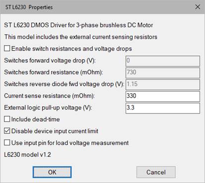
Current sense resistance (mOhm): Indicates the resistance value of the three-phase current sensing resistors. The output at v_Isense will then be Iout*Rsense for each of the three phases. Note that the sense resistors are included in the model.
Disable device input current limit: Disables the L6230 input (supply) current limit threshold of 2.8A typical.
Enable switch resistances and voltage drops: Enables the inclusion of the internal switches resistance and the switches voltage drop.
External logic pull-up voltage (V): Determines the output value at the VCPout and DIAG/ENout pins, assuming an internal pull-up.
Include dead-time: Enables the L6230 fixed dead-time of 1us.
Switches forward resistance (mOhm): Indicates the forward resistance of the half-bridge MOSFETs in milli-Ohms. The typical ON-resistance of the L6230 at 25°C is 730 milli-Ohms.
Switches forward voltage drop (V): Since the half-bridge switches are MOSFETs in the L6230, this value is typically 0V.
Switches reverse diode fwd voltage drop (V): Indicates the forward voltage of the integrated MOSFET reverse diodes in volts. This value is typically 1.15V at 1.4A output current for the L6230.
Use input pin for load voltage measurement: The load voltage measurement can be used to correctly represent the output phase voltages when both half-bridge switches are off (during the dead-time). If this parameter is not activated, the load voltage will be estimated during the dead-time transition assuming a balanced three-phase load.