AE Card
This card specifies an excitation at an edge between triangular surface elements.
On the Source/Load tab, in the Sources group,
click the ![]() Voltage source
icon. From the ドロップダウンリスト, click the
Voltage source
icon. From the ドロップダウンリスト, click the ![]() Voltage on edge (AE) icon.
Voltage on edge (AE) icon.
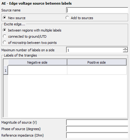
Figure 1. The AE - Edge voltage source between labels dialog.

Figure 2. Example of the use of the AE card.
Parameters:
- New source
- A new excitation is defined which replaces all previously defined excitations.
- Add to sources
- A new excitation is defined which is added to the previously defined excitations.
- Excite edge
- This specifies how the edge is determined:
- Meshed surface represents positive feed side
- By default, the feed direction is such that the meshed surface represents the negative feed side. The vector direction of the current is then towards the UTD or ground. When this option is checked, the feed orientation is reversed.
- Magnitude of source (V)
- Magnitude value of the voltage source in V.
- Phase of source (degrees)
- Phase of the voltage source in degrees.
- Reference impedance (Ohm)
- 励振の基準インピーダンスは、Sパラメータの計算用に使用されると共に、得られた利得の計算に使用される基準インピーダンスです。この基準インピーダンスは、POSTFEKO内で反射係数を計算して表示するために使用されるデフォルトの基準インピーダンスでもあります。Sパラメータの計算でこの欄が空白または0の場合は、SPカードで指定された値が使用されます。得られた利得と反射係数の計算でこの欄が空白または0の場合は、50オームが想定されます。
It should be noted that the edge between the surfaces with labels Negative side and Positive side does not have to be straight. It is possible, for example, to excite two half cylinders against each other. If an impedance must also be applied to the edge, the AE card can be combined with the LE card.
For the case where
the option, between regions with multiple labels, is selected more
than two surfaces may be connected to a feed edge. Examples for this as seen in the figures
are:
- one surface fed against three others
- two surfaces fed against two other surfaces
- and a feeding edge on a junction between three surfaces.

Figure 3. Example of a feed edge where more than one surface is connected on one side of the feed.

Figure 4. Example of a feed edge where more than one surface is connected on both sides (negative and positive) of the feed.

Figure 5. Example of a feed edge of three surfaces with different labels, where for instance label 2 could be fed against labels 1 and 3, but also label 1 could be fed against 2 and 3, or 3 could be fed against 1 and 2.