Extract Altium Designer ASCII file,
*.PcbDoc, in Altium Designer.
From the menu bar, click File > Import ECAD > Altium Designer.
The Import from Altium Designer dialog opens.
Layer Set-Up: Set Altium layers’ name which will be used as PDB’s
component outline layer, board outline layer and Drill Layer.
Use 0 for COC line width: Apply the line width of COC to zero.
Define Part Name: You can set the ECAD Part name as a Property or
Parameters value.
Property Keyword Name: Set the Part Name with the Design Item ID or
Footprint Name in Altium Designer design data.
Parameters Name: Set the ECAD Part Name with the parameter of Altium
Designer design data you specified.
Apply to Environment Setting: Apply settings to the environment
setting.
Select the target ASCII file, *.PcbDoc, to import.
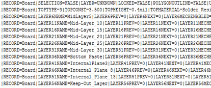
The format to
import Altium Designer is shown in Figure 1. Example of
*.PcbDoc. Figure 1.
The extension of Altium Protel 99 SE is the same with
*.pcb, but the format is the same as Altium Designer. You must import ASCII file using
Altium Designer menu.
Note: In Altium Designer,
you can save a file either binary or ASCII format with the same extension
(*.PcbDoc). You should import the ASCII format data
into PollEx.