Example 2: Design of an Array of Slotted Waveguides
This case explains how to create an array with 12 upper waveguides and calculate its far-field, radiation pattern, current density, charge density and near field.
Step 1 Create a New MOM Project
Open ' newFASANT' and select ' File --> New' option.
Figure 1. New Project panel
Select ' MOM' option on the previous figure and start to configure the project.
Step 2Change the scale to cm.
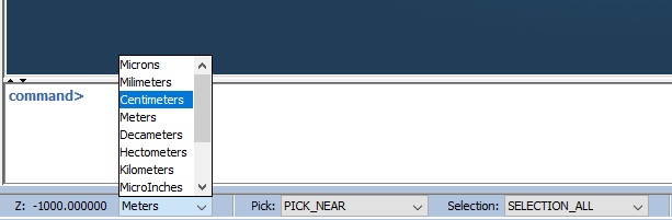
Figure 2. Scale settings
Step 3Open the function
Select ' Tools --> User Functions' option on the menu bar and open the function "SlottedWaveguideArray .java"
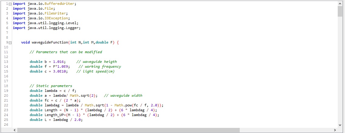
Figure 3. User Function Code
Look at these lines, where you can change the parameters of the waveguide structure
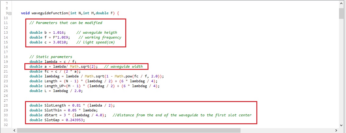
Figure 4. User Function Code
The parameter "a" represents the width of the guides and is calculated to be equal to lambdag / 2 so that for any working frequency the side walls of the upper guides are in contact and there is no gap.
Step 4Create the geometry of the waveguide array
Select ' Tools --> Calculator' option on the menu bar and write "SlottedWaveguideArray(N,M,F)".
In our case, as we want a 12-slot feeding waveguide, N= 12, M=11 and F is the working frequency value in GHz.
The script file, called “ script_waveguide.nfs”, will be automatically generated in the mydatafiles folder in the newFASANT directory.
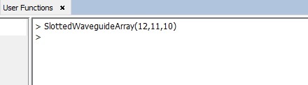
Figure 5. Calculator panel
So our array will have a feeding waveguide with 12 slots, 12 upper guides with 11 slots each one and the working frequency is 10 GHz.
Step 5Load the generated Script
The next step is to execute the generated script file. For that, click on Tools – Script - Load and open the script "script_waveguide.nfs".
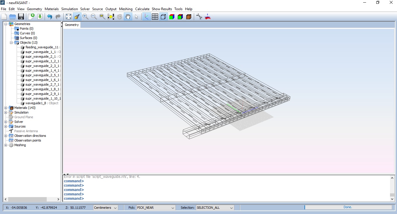
Figure 6. Geometry
Step 6Set Simulation Parameters
Select ' Simulation --> Parameters' option on the menu bar and the following panel appears. Set the parameters as the next figure shows and save it.
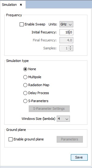
Figure 7. Simulation Parameters panel
If the frequency to which you are going to simulate is equal to the frequency at which the parameters of the array were calculated, the radiation diagram will have the shape of a brush pointing along the z axis. On the other hand slightly varying the frequency of simulation will get the brush to oscillate around the z-axis.
Step 7Add a port to the feeding waveguide.
Click on the waveguide and Select ' Source --> Waveguides--> Add Waveguide Port' option on the menu bar and add the port (see Add Waveguide Port).
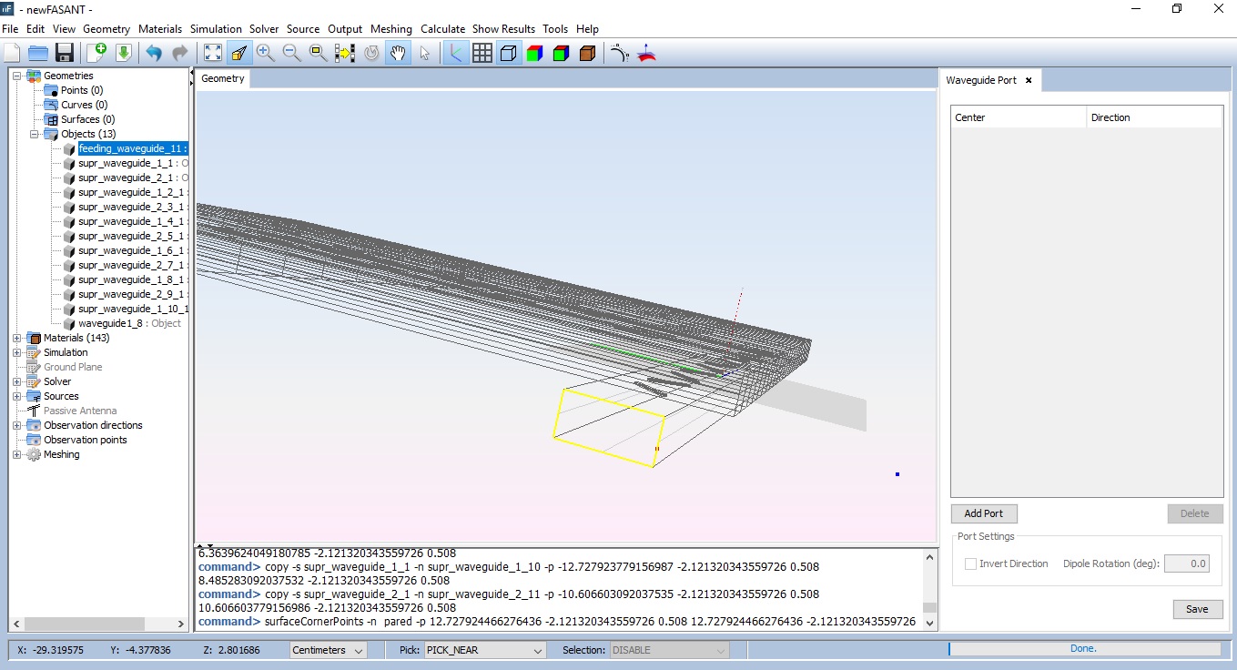
Figure 8. Add Waveguide Port Panel
Step 8 Set the solver parameters.
Click on Solver --> Parameters option on the menu bar. Verify that all the parameters are defined by default, as shown in next figure. Click on Save button before going to next step
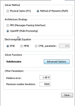
Figure 9. Solver panel
Select ‘ Advanced Options’ and activate Preconditioner as shown.
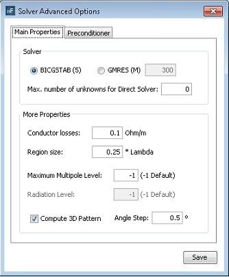
Figure 10. Main Properties Solver Panel
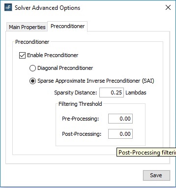
Figure 11. Preconditioner Solver Panel
Step 9Meshing the geometry model.
Select ' Meshing --> Parameters' to open the meshing configuration panel and then set the parameters as show the next figure. In order to obtain the shortest possible time for meshing, it is recommended to run the process of meshing with the number of physical processors available to the machine. As it is a very complicated design requires 20 divisions in the mesh and a high computing capacity
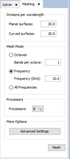
Figure 12. Meshing Panel
Step 10Execute the simulation.
Select ' Calculate --> Execute' option to open simulation parameters. Then select the number of processors as the next figure show. In order to obtain the shortest possible time for calculating the results, it is recommended to run the process with the number of physical processors available to the machine.
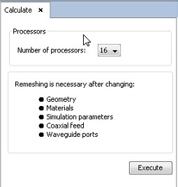
Figure 13. Execute panel
Then click on ' Execute' button to starting the simulation.
Step 11Show Results.
To get more information about the graphics panel advanced options (clicking on right button of the mouse over the panel) see Annex 1: Graphics Advanced Options.
Select ' Show Results --> Radiation Pattern --> View 3D Pattern' option to show the radiation diagram in three dimensions.
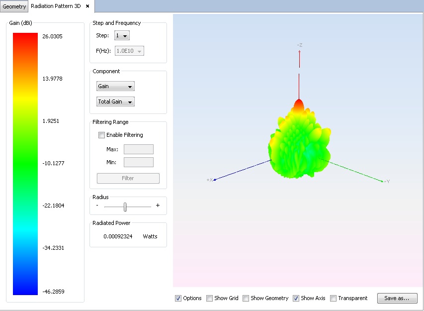
Figure 14. 3D Radiation Pattern
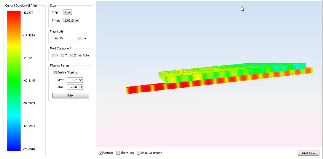
Select ' Show Results --> View Currents ' option to show the current density on the surfaces of the array.