Creating the Model
Create the model in CADFEKO. Define any ports and sources required for the model. Specify the operating frequency or frequency range for the model.
- Set the model unit to millimeters.
-
Define the following variables:
- d = 5.8 (The spacing for the periodic boundary condition.)
- h = 0.5 (The thickness of the substrate.)
- t = 0.091 (The thickness of the bonding material.)
- s1 = 0.15 (The width of the dielectric surface, bottom layer.)
- s2 = 0.18 (The width of the dielectric surface, upper layer.)
- w = 2.5 (The width of the centre metallic surface.)
- fmin = 5e9 (The minimum frequency.)
- fmax = 15e9 (The maximum frequency.)
-
Create the two layers for the dielectric.
-
Create a cuboid for the lower layer centred at the origin.
- Definition method: Base centre, width, depth, height
- Base centre: (0, 0, 0)
- Width: d
- Depth: d
- Height: h
- Label: LowerLayer
-
Create a cuboid for the middle layer.
- Definition method: Base centre, width, depth, height
- Base centre: (0, 0, h)
- Width: d
- Depth: d
- Height: t
- Label: Glue
-
Create a cuboid for the upper layer.
- Definition method: Base centre, width, depth, height
- Base centre: (0, 0, h + t)
- Width: d
- Depth: d
- Height: h
- Label: UpperLayer
-
Create a cuboid for the lower layer centred at the origin.
-
Create the lower and upper PEC surfaces.
-
Create the upper rectangle.
- Definition method: Base centre, width, depth
- Base centre: (0, 0, h + t + h)
- Width: d-s1
- Depth: d-s1
- Label: S1
-
Create the lower rectangle.
- Definition method: Base centre, width, depth
- Base centre: (0, 0, 0)
- Width: d - s2
- Depth: d - s2
- Label: S2
-
Create the upper rectangle.
-
Create the outline of the PEC surface on the bonding material.
-
Create a rectangle.
- Definition method: Base centre, width, depth
- Base centre: (0, 0, h + t)
- Width: d
- Depth: w
- Label: L1
-
Create a rectangle.
- Definition method: Base centre, width, depth
- Base centre: (0, 0, h + t)
- Width: w
- Depth: d
- Label: L2
-
Create a rectangle.
- Union the parts, L1 and L2.
- Use the Simplify transform on Union1 to remove redundant edges caused by the overlapping of two rectangles.
- Union all the parts.
-
Create the two dielectric media.
-
Create the dielectric medium, Substrate.
- Relative permittivity: 3.38
- Dielectric loss tangent: 0
- Label: Substrate
-
Create the dielectric medium, Glue.
- Relative permittivity: 3.3
- Dielectric loss tangent: 0
- Label: Glue
-
Create the dielectric medium, Substrate.
-
Set the region properties of the two layers.
- Set the region of the middle layer to Glue.
- Set the region of the remaining two layers to Substrate.
-
Set the face centred on top of the Glue material to
PEC.
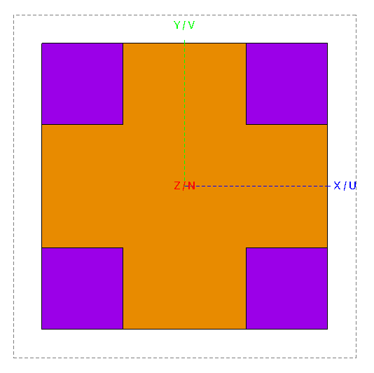
Figure 1. Top view of the FSS using a cutplane to show the face centred on top of the glue material set to PEC (indicated in orange). -
Set the large top face and large bottom face to PEC, but keep the remaining
narrow faces (which border the large top face and bottom face respectively) set
to Default or Dielectric
boundary.
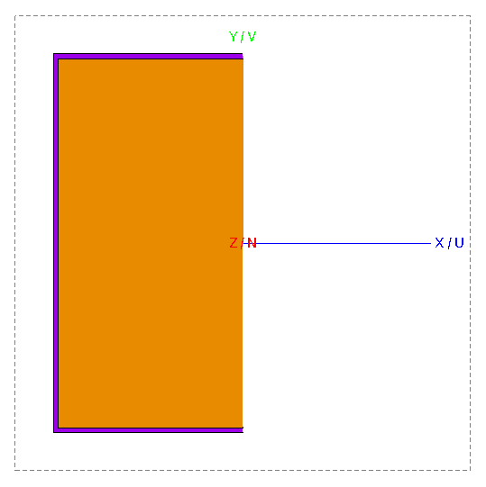
Figure 2. Top view of the FSS. The top face and bottom face are set to PEC (indicated in orange). The narrow top face and bottom face are not set to PEC (indicated in purple). - Add a single incident plane wave with θ=0° and ϕ=0°.
- Set a continuous frequency range from fmin to fmax.
-
Specify the symmetry about 2 principal planes:
- X=0: Geometric symmetry
- Y=0: Geometric symmetry
Note: Only geometric symmetry is supported for periodic boundary conditions.