Key Pad
Check the key pad design and via usages.
This section examines contents related to the key pad used in mobile phone design.
Because key pads are also used with a via, location of vias are
important.
- Key Pad Target Component Definition
- Target Component Selection: Select the target components with key
pads from the component group list.
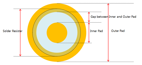
Figure 1.
- Target Component Selection: Select the target components with key
pads from the component group list.
- Checking
- Check Via at the Center of Inner Pad: Checks the via location in
the inner pad. If it is located at the center of inner pad, it is a
fail.
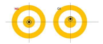
Figure 2. - Check Via in Gap between Inner and Outer Pad: Checks whether vias
are in the gap between the inner and outer pad. If it is located at
the gap area, it is a fail.
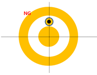
Figure 3. - Existence of Solder Mask: Checks the existence of solder masks and
if there is no solder mask, it is a fail.
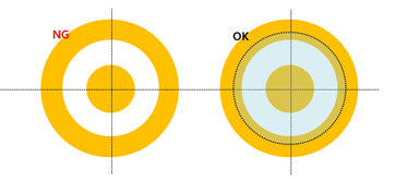
Figure 4. - Silkscreen near Key Pad: If the silkscreen is overlapped with the
pad, it is a fail.
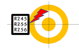
Figure 5. - Allowable Maximum Via Hole Size: Set the maximum size of the via hole.
- Via Alignment: Check the via alignment, if they are not aligned,
they fail.
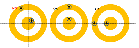
Figure 6. - Number of Vias in Inner Pad: Set the number of vias in the inner pad. If the number of inner pads is not matching with the given value, it is a fail.
- Number of Vias in Outer Pad: Set the number of vias in the outer pad. If the number of inner pads is not matching with the given value, it is a fail.
- Check Via at the Center of Inner Pad: Checks the via location in
the inner pad. If it is located at the center of inner pad, it is a
fail.