All Components: All components on design will be target
components.
Exclude Components: Among all components, select void-checking
components from component group list.
Component Group Selection: Select target components from component group
list.
Checking
Check Co-Existence for Metal Mask and Solder Mask: For target
components, check all pads have metal mask and solder mask. One of them
doesn’t exist, it is fail.
Check matching for Metal Mask and Solder Mask: Option to check
whether the size of the Metal Mask and the Solder Mask
match.
Include DIP Component: Option to check whether the Metal Mask
exists on Pad of Through Hole type component.
Metal Mask Existence:
DIP Component Checking Condition: Option to check whether the
Metal Mask exists for the Through Hole type components.
Component Placed Side: Option to check whether the Metal Mask
exists on the pad of the component placed side.
Reverse Side: Option to check whether the Metal Mask exists on
the pad of the opposite side.
Both Side: Option to check whether the Metal Mask exists on the
pad of the both sides.
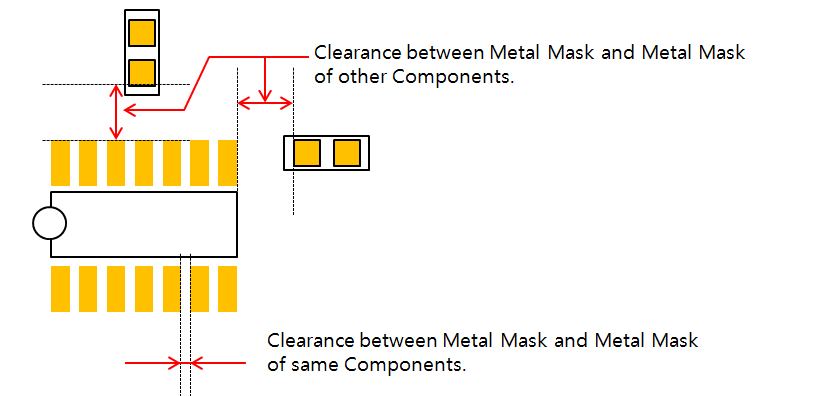
Clearance between Metal Mask in same Component: Set the clearance value
between metal masks in same components pads.
Clearance between Metal Mask and Objects on certain Layers: Check the
clearance between metal mask and objects placed on certain layers.
Layer Selection: Select layer from layer list. All objects on
selected layer will be target objects.
Clearance: Set the clearance value between metal mask and
objects on selected layer.
Clearance between Metal Mask and Other Component’s Metal Mask: Set the
clearance value between metal mask and metal masks in other
components.
Figure 1.
Clearance between Metal Mask and Other Component’s Solder Mask: Check
the clearance between metal mask and solder mask in other
components.
Top Solder Mask Layer: Select top solder mask layer from layer
list. Default is layer number three of PollEx PCB data structure.
Bottom Solder Mask Layer: Select bottom solder mask layer from
layer list. Default is layer number 13 of PollEx PCB data structure.
Clearance: Set the clearance value.
Clearance between Metal Mask and Via: Clearance checking between Metal
Mask and Via.
Exclude Thermal Pad: Option to exclude the Thermal Pad from
clearance checking between Metal Mask and Via. Select a
component group including the thermal pad.
Clearance between Metal Mask and Hole: Clearance checking between Metal
Mask and Hole.