OS-T: 1100 Thermal Stress Analysis of a Printed Circuit Board with Anisotropic Material Properties
Printed Circuit Boards (PCB's) are used in electronic components to both mechanically support and provide electrical connections between components. Construction involves etching a thin copper layer that has been deposited onto a non-conductive, glass-fiber/epoxy composite substrate. Electrical components are then mounted to the board and connected to the copper traces with electrical solder.
The concentrated, intense heating that occurs during the soldering process creates stresses in the substrate material. In this exercise, you will simulate this process and determine if the stresses and strains resulting from this process are acceptable or not.
The model makes use of solid hexahedral (CHEXA8) elements with a thin skin of shell elements (CQUAD4) on the outside faces.
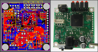
Figure 1.
Launch HyperMesh and Set the OptiStruct User Profile
Open the Model
Set Up the Model
Create MAT9 Material for Solid Elements
- Enter the following values for the thermal expansion rates and reference temperature:
- A1
- 1.6e-5
- A2
- 1.9e-5
- A3
- 8.0e-5
- TREF
- 10.0
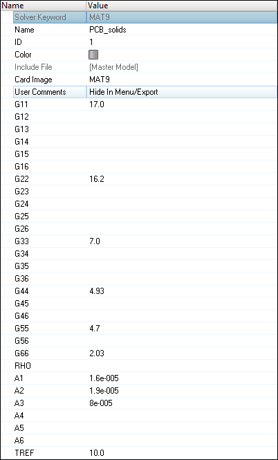
Figure 2.
Create MAT2 Material for Shell Elements
Create Properties with a Material Reference
-
Enter the thickness for the shell component by clicking
T, and enter 0.001.
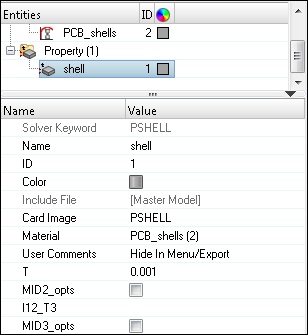
Figure 3.
Create Displacement Constraints at the Mounting Holes
- Select a suitable color.
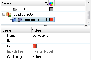
Figure 4.
Create Applied Temperature Loads at the Solder Pads
- Create a new load collector named temperature_loads.
- Leave Card Image set to None.
- Click to open the Temperatures panel.
- Click .
- Check the box next to the solder_pads component.
- Click select.
- Verify that constant value (the field label specifies value=) is selected and enter 345.0.
- Verify the load types= is set to TEMP.
- Click create to create the temperature_loads.
- Click return to go back to the main menu.
Create a Load Step
Add Control Cards to the Analysis
Submit the Job
-
From the Analysis page, click the OptiStruct
panel.
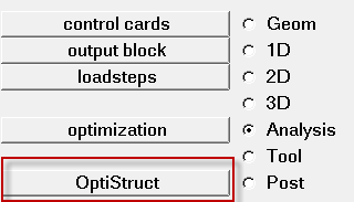
Figure 5. Accessing the OptiStruct Panel